Home / PCB design And Service
We Engineer Your Vision
Schematic Design
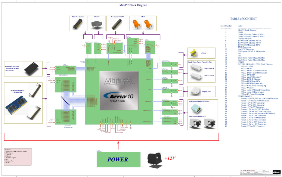
Analog / Digital schematics with best practices.
PCB Layout
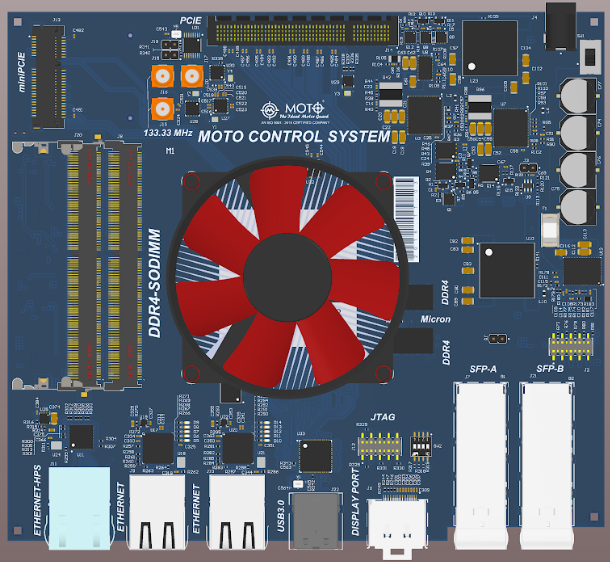
1–6-layer boards with impedance control.
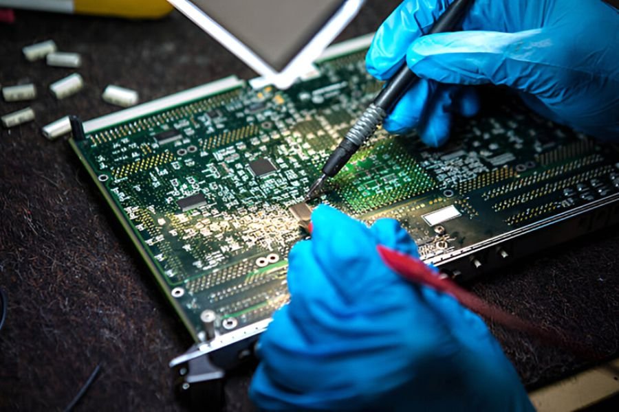
Fabrication
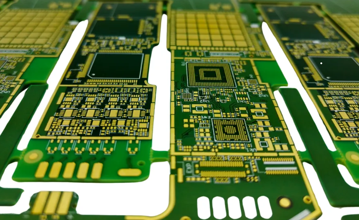
Turnkey PCB manufacturing & assembly.
Technical Highlights
Up to 6 layers
3–10 mil (down to 2 mil for HDI)
IPC-2221\IPC-7351 Compliance
Our Services
PCB Design & Layout
- Reverse engineering
- Schematic Capture & Netlist
- Bom generation
- Multi-layer Design (up to 6 layers)
- High-speed signal routing (DDR, HDMI, USB, RF)
- DFM/DFT checks
- Design tools: Altium, OrCAD, EasyEDA
- All designs follow IPC standards including: IPC-2221, IPC-7351, IPC-6012

PCB Manufacturing
- Board Types: Rigid, Flex, Rigid-Flex
- Material Options: FR4, FR4BLACK, MCPCB
- Layer Count: 1–6 layers
- Board Thickness: 0.3 mm – 3.2 mm
- Copper Thickness: 1 oz – 3 oz
- Min Trace/Space: 3 mil / 3 mil
- Min Hole Size: 0.5 mm
- Surface Finish: HASL, ENIG, Immersion Silver/Gold, lead free
- Quality Standards: IPC Class 2 & 3, ISO 9001, RoHS compliant
PCB Assembly
- Tech: SMT, THT, Mixed
- Components: 0603 to LQFN, TQFN, SOIC, SOP
- Testing: AOI, ICT, Functional Testing, Flying probe

LET’S TALK ABOUT YOUR VISION
Call us: +91 97861 34445, +91 97862 34445
Email: info@motocontrolsystem.com